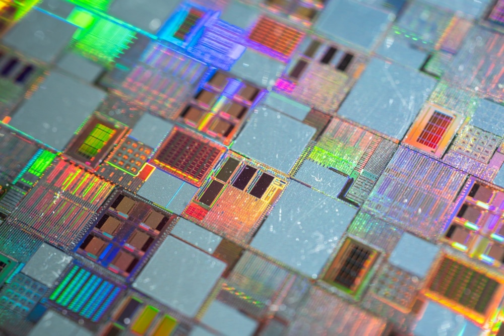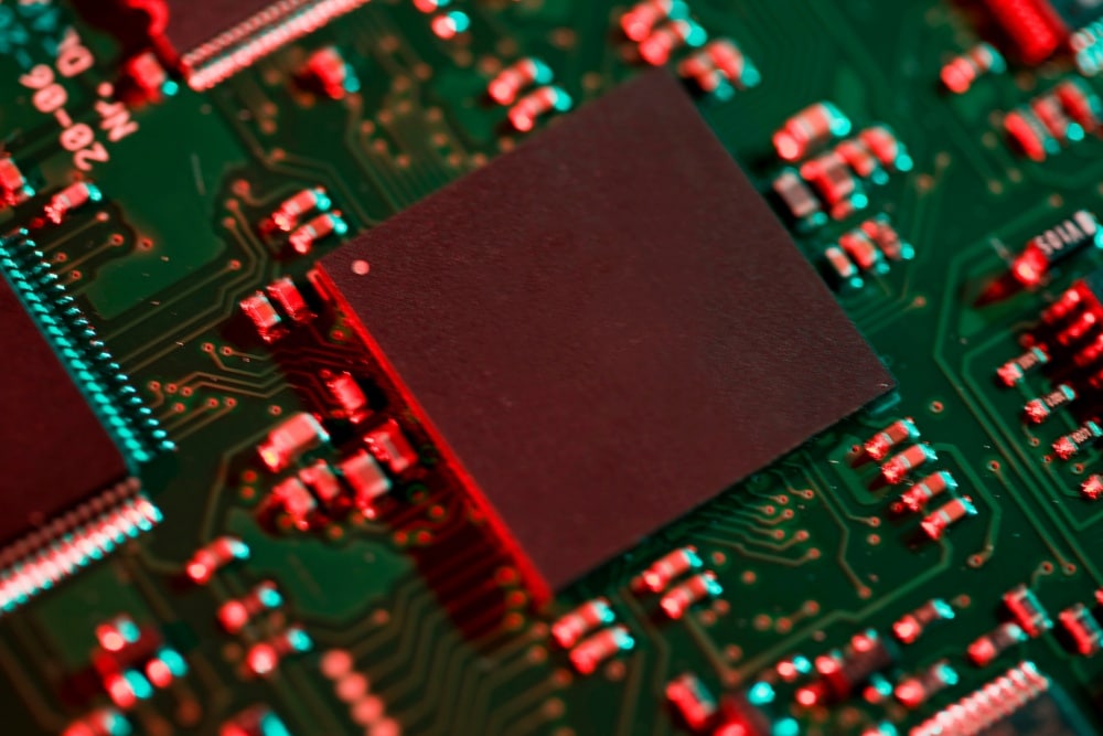
Heterogeneous Integration: Elevating Semiconductor Functionality
As the limits of traditional semiconductor scaling become more pronounced, heterogeneous integration (HI) is emerging as a key enabler of continued innovation. By combining diverse materials and components—each selected for optimal performance in specific roles—HI overcomes the constraints of single-platform architectures. It facilitates the integration of functions that no single photonic or electronic platform can deliver alone, unlocking new capabilities in performance, size, and efficiency.
This approach is not simply additive; it allows for purposeful combinations of silicon, III-V materials, and specialised substrates to achieve design goals that would be otherwise unattainable. Whether the objective is to reduce power consumption, boost data transmission speed, or introduce new sensing capabilities, heterogeneous integration provides the architectural flexibility required by next-generation devices.
Its impact is already evident across sectors, from miniaturised wearables and advanced imaging systems to high-performance optical transceivers and emerging compute architectures. These diverse applications share a common demand: the seamless integration of specialised materials and components to meet increasingly stringent performance, power, and form-factor requirements.
As systems grow more data-intensive and latency-sensitive, the ability to co-design and co-package disparate technologies is no longer optional—it is fundamental. And when it comes to heterogeneous integration, it moves beyond incremental improvement. Instead, it establishes the structural framework for the semiconductor systems of tomorrow.
A New Paradigm for Chip Design
What happens when no single material or technology can meet the growing demands of performance, power efficiency, and compactness?
The answer lies in rethinking how chips are designed and assembled.
Traditional methods, limited by the constraints of a single substrate, are giving way to more flexible, cross-material architectures that enable more capability in less space. Heterogeneous integration has emerged as a critical enabler, driving this shift across industries.
Defining Multi-Component Integration
Heterogeneous integration refers to the strategic assembly of diverse semiconductor components, materials, and technologies into a unified system—either on a single substrate or through tightly coupled multi-chip modules. Unlike monolithic integration, which fabricates all functions using a single material system such as silicon, HI brings together multiple elements with distinct physical and electrical properties to perform optimally as a collective whole.
This architectural shift allows device designers to select the best material for each function—such as III-V semiconductors for high-speed optics, or GaN for power handling—and combine them using advanced bonding techniques.
Key processes include wafer bonding, die-to-wafer (D2W) hybrid bonding, and through-silicon vias (TSVs), each offering precise vertical and lateral alignment between layers or chiplets. These methods facilitate efficient communication pathways, reduce interconnect length, and allow for higher integration density without sacrificing thermal or signal performance.
The functional building blocks in HI may include silicon photonics devices, post-processed CMOS chips, or advanced photonic integrated circuits. Through precise co-packaging, components that were once isolated by substrate or manufacturing constraints can now operate synergistically—each optimised for its task, yet fully interoperable.
Fundamental Importance in Contemporary Devices
As mentioned, by integrating diverse components—processors, memory, photonics, sensors, and power amplifiers—on a common substrate or within a tightly coupled package, HI enables systems to achieve higher speeds, reduced form factors, and improved thermal efficiency.
This architecture provides design teams with greater flexibility to tailor functionality to specific application demands. For instance, it can allow for the combination of high-performance digital cores with low-power analogue elements or specialised accelerators, delivering differentiated performance without compromising energy budgets. This modularity also shortens development cycles, offering a practical path for system-level optimisation across a variety of use cases.
Energy efficiency is a core advantage as well.
By shortening interconnect distances and minimising parasitic losses between subsystems, HI contributes to meaningful reductions in power consumption and heat dissipation—both of which are critical for mobile, edge, and data-intensive platforms.
Simply put, as demand grows in areas such as autonomous systems, advanced driver-assistance, wearables, and medical diagnostics, HI provides the foundation for integrating complex functionalities into increasingly compact, reliable, and high-performing devices.
Core Technologies Driving Integration
So, which technologies are shaping the next generation of advanced semiconductor systems?
At the heart of heterogeneous integration lies a suite of precision engineering techniques that enable the seamless combination of materials, processes, and components. Some of these include:
1. Layered Chip Architectures (Monolithic 3D Integration)
Monolithic 3D integration introduces a vertically stacked chip structure, enabling dense and efficient use of silicon real estate. By placing multiple active device layers directly atop one another on a single wafer, this architecture shortens signal paths between functional blocks, significantly enhancing intra-chip communication speed and reducing latency.
The use of precise alignment markers during the stacking process ensures tight inter-layer registration, which not only optimises logic-to-memory bandwidth but also minimises thermal overheads. These benefits translate into improved energy efficiency, reduced packaging volume, and higher integration density.
Efficient On-Chip Data Routing (Network-on-Chip Architectures)
As chip complexity increases, traditional point-to-point wire connections become a bottleneck for data exchange. Network-on-Chip (NoC) architectures resolve this by establishing a scalable data-routing framework within the chip itself. Instead of relying on static interconnects, NoCs implement a grid-like topology—complete with routers and links—enabling multiple chip components to exchange information concurrently and efficiently. This is especially critical for systems handling massive parallel processing, such as those found in AI accelerators, autonomous vehicles, and real-time edge computing, where reliable, high-speed internal communication is essential.
Multi-Material Light Guides (Heterogeneous Waveguide Systems)
Heterogeneous waveguide systems leverage multiple materials with distinct optical properties to guide light precisely across integrated chips. These light channels are engineered to transmit data using photonic signals, resulting in significantly faster transfer speeds and lower power draw compared to conventional electronic interconnects.
By incorporating low-loss, high-index contrast materials within defined cavity regions, these systems reduce signal interference and maintain transmission integrity even at high data rates. This makes them particularly well-suited for high-throughput environments such as data centres, edge computing, and photonic AI accelerators.
Diverse Applications Fueled by HI
Now, how exactly is heterogeneous integration advancing real-world innovation?
By enabling the seamless combination of specialised chip components on a single platform, its growing adoption across sectors, especially those requiring compact, high-efficiency systems, is driving breakthroughs in electronics, healthcare, and connected devices.
Advanced Material Blending
The integration of Gallium Nitride (GaN) and other III-V semiconductors with silicon substrates marks a significant advancement in chip engineering. These wide-bandgap materials offer high electron mobility and superior thermal characteristics, making them ideal for power-intensive applications. When used in conjunction with silicon vias and hybrid bonding techniques, GaN and III-V elements enable devices that deliver faster switching speeds, improved heat dissipation, and lower energy draw.
Modular Designs for Specialised Uses
Chiplet-based architectures are enabling a new wave of domain-specific designs tailored for applications with unique performance, size, and reliability requirements.
In the medical technology sector, modular chip configurations allow for precise customisation, combining multiple silicon functions such as sensing, data processing, and wireless communication into a single compact unit. This modularity supports faster signal processing and real-time patient monitoring in diagnostics and implantable devices.
Wearable technology is another area benefiting from HI-driven modularity. Post-processed CMOS chips and advanced wafer bonding are being employed to maximise functionality while reducing power consumption—key for devices constrained by form factor and battery life.
Pioneering Advancements in HI

Building on its diverse applications, heterogeneous integration continues to drive critical innovation in semiconductor design.
Quantum Information Processing
Quantum integrated photonics is emerging as a cornerstone of high-performance computing systems.
By leveraging light for information transfer, these platforms enable significantly faster signal propagation and reduced interference compared to traditional electrical connections. Through the use of silicon wafers and hybrid bonding—rather than conventional wire bonding—designers can build more stable and scalable quantum systems.
Next-Generation Transistor Designs
Complementary FET (CFET) technology is enabling a new class of ultra-compact transistor structures. Stacking n-type and p-type transistors vertically allows for reduced footprint while maintaining electrical isolation and alignment precision. This architecture lowers power requirements and improves integration density—key factors for sustaining high-speed communication across advanced chip systems.
Meanwhile, ferroelectric FETs (FeFETs) are gaining traction for their ability to store data within the transistor structure itself. Utilising ferroelectric materials, these devices provide faster switching times and retain data with minimal power draw. When integrated into post-processed CMOS platforms, FeFETs offer an effective route to combine non-volatility, low energy usage, and enhanced processing capability.
Overcoming Integration Hurdles and Future Prospects
As heterogeneous integration pushes the boundaries of what’s possible in chip design, the complexity of aligning materials, processes, and systems becomes increasingly apparent. Addressing these challenges with precision and foresight is key to unlocking the next wave of semiconductor innovation.
Key Technical and Material Challenges
Achieving seamless integration demands micron-level alignment and careful thermal management to prevent material degradation. Therefore, advanced techniques like hybrid bonding and through-silicon vias must be tightly controlled to ensure performance is not compromised.
Material compatibility also presents hurdles as the differing thermal and electrical behaviours of combined substrates can disrupt communication paths, reduce reliability, or lead to system inefficiencies if not precisely engineered.
Economic and Scalability Considerations
Scaling heterogeneous integration is a capital- and talent-intensive effort. It demands substantial investment in advanced equipment and highly specialised design and prototyping expertise. Moving from lab-scale breakthroughs to high-volume manufacturing introduces complex challenges around yield, process stability, and cost control. To drive broader adoption, the industry must strike a careful balance between performance, reliability, and commercial viability.
Emerging Directions and Opportunities
The evolution of heterogeneous integration is already reshaping edge computing. With reduced latency and thermal demands, systems can now support increasingly complex workloads directly at the edge.
In deep learning, HI facilitates tighter chip-to-chip communication, allowing for more efficient execution of large-scale neural networks. Hybrid bonding techniques and new transistor architectures make it possible to build systems optimised for high-throughput, low-power inference and training—core needs for next-generation AI applications.
To support these developments, Electronic Design Automation (EDA) tools must evolve.
Traditional design environments are not equipped to handle the precision requirements of wafer-level bonding or multi-material integration. The next frontier in EDA involves simulation and validation platforms that can model mechanical stress, alignment tolerances, and thermal interactions across 3D structures. These advancements will be critical in translating theoretical designs into manufacturable, scalable systems.
NSTIC’s Leadership in Heterogeneous Photonics Integration
As demand intensifies for higher data throughput, lower latency, and improved energy efficiency across industries, NSTIC is advancing photonics integration to meet these challenges.
By developing next-generation photonics technologies through novel material integration and wafer-level capabilities, NSTIC strengthens Singapore’s position as a strategic hub for semiconductor innovation.
Driving Next-Generation Photonics
To address the performance limitations of current silicon photonics, NSTIC is advancing photonic heterogeneous integration (PHI) to support transceivers operating beyond 3.2 terabits per second and next-generation optical interconnects. This strategy integrates high-performance materials—including III-V lasers and semiconductor optical amplifiers, lithium niobate modulators, barium titanate, and ultra-low-loss deuterated silicon nitride—onto silicon substrates.
By leveraging 8-inch and 12-inch wafer-level fabrication via die-to-wafer bonding, NSTIC positions silicon as the foundational platform for scalable photonic systems. These developments enable higher bandwidth, improved energy efficiency, and greater functionality for applications in AI, data centres, and telecommunications.
Accelerating Translation and Ecosystem Growth
NSTIC supports the full spectrum of photonics R&D with access to a 300mm wafer cleanroom, advanced semiconductor tools, and domain expertise. Companies and researchers can accelerate prototyping, testing, and small-volume production with streamlined paths to commercial foundries. Beyond infrastructure, NSTIC fosters an ecosystem of collaboration—facilitating IP licensing, fee-for-service engagements, and the upskilling of local talent to meet evolving industry demands.
Explore partnership opportunities with NSTIC to advance photonics innovation with greater speed, precision, and scalability.
