Flat Optics & Metalens Technology | Metaoptics Solutions
Flat Optics Technology: Revolutionising Opticswith Metalens & Metaoptics
Flat optics technology is a disruptive force set to redefine modern photonics. This emerging field, which includes the broader science of metaoptics and the revolutionary metalens, enables the development of ultra-compact, high-performance optical systems, marking a significant departure from the limitations of traditional bulk optics.
TABLE OF CONTENTS
- What is Flat Optics?
- Metalens & Metaoptics: The Future of Photonics
- Why Flat Optics? Unparalleled Benefits for Next-Generation Devices
- Transforming Industries: Applications Powered by Flat Optics
- Your Partner in Flat Optics Innovation: NSTIC’s Comprehensive Capabilities
- Collaborative Innovation: The NSTIC Advantage in Flat Optics
- Ready to Innovate? Connect with Our Flat Optics Experts
What is Flat Optics?
Flat Optics (a.k.a metaoptics) is a game-changing technology that will revolutionise the industry by significantly reducing the size, weight and cost of imaging and sensing devices while adding advanced wide-ranging functionalities that are currently unavailable.
It manipulates light using precisely engineered thin, planar surfaces, rather than thick, curved glass. These surfaces are patterned with features smaller than the wavelength of light, known as nanostructures, which function as advanced optical elements. By meticulously designing these patterns, it becomes possible to control the fundamental properties of light—including phase, amplitude, and polarisation—with unprecedented spatial resolution.
This capability allows a single, thin component to perform complex functions that would traditionally require multiple bulky lenses, heralding a new era in the design and fabrication of optoelectronic devices.
Key advantages
- Miniaturisation
- Reduction in weight
- Reduction in the number of optical components
- Multi-functionality
- Mass producible
Metalens & Metaoptics: The Future of Photonics
The field of metaoptics, also known as nanophotonics, centres on manipulating light at a sub-wavelength level through the design, fabrication, and application of engineered structures, commonly referred to as metasurfaces.
A metalens is a flat metasurface composed of an array of precisely arranged optical nano-elements. These individual elements work together to shift the phase of incoming light locally. This collective action allows the metalens to reshape a light wave, enabling it to perform complex focusing and imaging tasks traditionally handled by larger, curved lenses.
Together, metaoptics and the metalens are what represent the future of the industry, unlocking new frontiers in system design by enabling lighter, more compact, and more powerful devices for applications ranging from consumer electronics to advanced scientific instrumentation.
Why Flat Optics? Unparalleled Benefits for Next-Generation Devices
Flat optics offer unparalleled benefits, making the next-generation devices significantly smaller, more cost-effective, and capable of higher performance than ever before.
- Miniaturisation & Weight Reduction: This technology facilitates profound miniaturisation and weight reduction by replacing complex, multi-element lens assemblies with a single, ultra-thin flat optic. It enables the integration of advanced optical functionalities into compact systems where space and weight are critical design constraints.
- Cost Efficiency & Mass Production: By leveraging established semiconductor manufacturing processes, such as those utilised in our 300mm wafer cleanroom, flat optics can be mass-produced on a wafer scale. This approach dramatically reduces production costs compared to traditional methods, enabling high-volume fabrication of thousands of lenses simultaneously.
- Enhanced Functionality & Performance: Flat optics enables components with enhanced, often multi-functional, performance. Precise control over light at the nanoscale allows for superior imaging quality with advanced aberration correction and the creation of novel optical functions previously unattainable with conventional components.
- Integration & Stability: The planar form factor of flat optics technology simplifies system integration, reducing alignment complexity and enhancing mechanical stability. Built for durability, these components deliver consistent and dependable performance under diverse operating conditions, making them ideally suited for challenging automotive, industrial, and commercial applications.
Transforming Industries: Applications Powered by Flat Optics
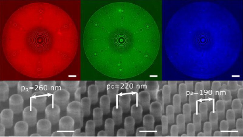
RGB metalenses 200um in diameter and SEM images showing nanostructures on the lenses
The revolutionary potential of flat optics and metalens technology extends far beyond theoretical concepts, now actively driving innovation across a multitude of high-tech industries. By replacing bulky, conventional lenses with ultra-thin metasurfaces, this technology is enabling the development of next-generation systems with previously unattainable performance and form factors.
- Imaging & Sensing: In imaging and sensing, flat optics enables extreme miniaturisation for radically thinner smartphone cameras and lighter AR/VR headsets. This technology also facilitates the development of compact drones, discreet security systems, and more miniature, minimally invasive biomedical endoscopes for advanced diagnostics.
- 3D Sensing: Flat optics technology provides superior control over light, significantly enhancing the signal-to-noise ratio for applications such as facial recognition. 3D mapping can now be faster, more accurate, and highly reliable for secure authentication and advanced interactive systems.
- Automotive: Flat optics enables the creation of highly compact optical systems for ADAS and autonomous vehicles. The miniaturisation simplifies the integration of essential cameras and LiDAR sensors, meeting the stringent performance, aesthetic, and reliability demands of modern vehicles.
- Advanced Light Manipulation: Beyond standard imaging, flat optics provides unprecedented control over light’s fundamental properties. This paves the way for novel devices, such as miniature spectrometers for portable chemical analysis and compact systems that provide advanced polarisation imaging for materials science and medical diagnostics.
Your Partner in Flat Optics Innovation: NSTIC’s Comprehensive Capabilities
As a leader in semiconductor photonics technologies, NSTIC provides flat optics research and development, along with deep expertise in metalens technology, to enhance research and development outcomes and transform ambitious concepts into market-ready realities.
From Concept to Blueprint: Advanced Optical Design & Simulation
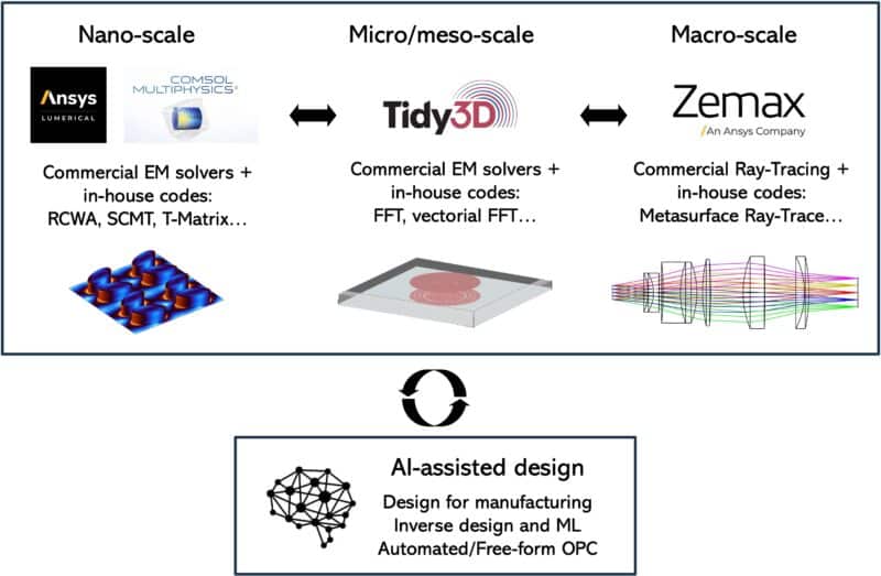
NSTIC’s design process transforms an initial concept into a validated manufacturing blueprint, underpinned by a rigorous approach to simulation and validation. We provide end-to-end support, leveraging a robust suite of industry-standard and proprietary tools to solve the most complex optical design challenges and ensure performance is optimised for fabrication.
End-to-End Design Scope:
- Full support for system, module, and individual component level design.
Advanced Simulation Toolkit:
- Nanoscale EM Solvers: Ansys Lumerical, COMSOL Multiphysics
- Ray Tracing: Ansys Zemax
- Proprietary In-House Code: Utilising Fourier Analysis, Rigorous Near-to-Far-field transformation, and Rigorous Coupled Wave Analyses (RCWA)
- AI-Assisted Inverse Design: Applied for engineering novel, large-scale, and multilayer flat optics
Pioneering Fabrication: Advanced Materials & Manufacturing Processes
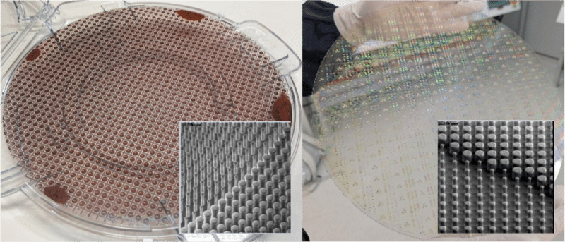
Our advanced, wafer-scale manufacturing processes bring optimised designs to life with exceptional precision and control. This expertise extends across a diverse portfolio of materials and sophisticated processing techniques, enabling us to fabricate high-performance flat optics tailored to specific spectral ranges and functional requirements.
Established Material Platforms:
- Ge/Si & a-Si/Si metalenses for the mid-IR spectrum
- a-Si/glass metalenses for the near-IR spectrum
- SiN/glass metalenses for the visible spectrum
Advanced & In-Development Capabilities:
- Double-sided wafer processing for dual-function optics
- In development: TiO2/glass metalenses for the visible spectrum
- In development: Multilayer processing for next-generation, multi-functional metalenses
Ensuring Excellence: Rigorous Testing & Characterisation
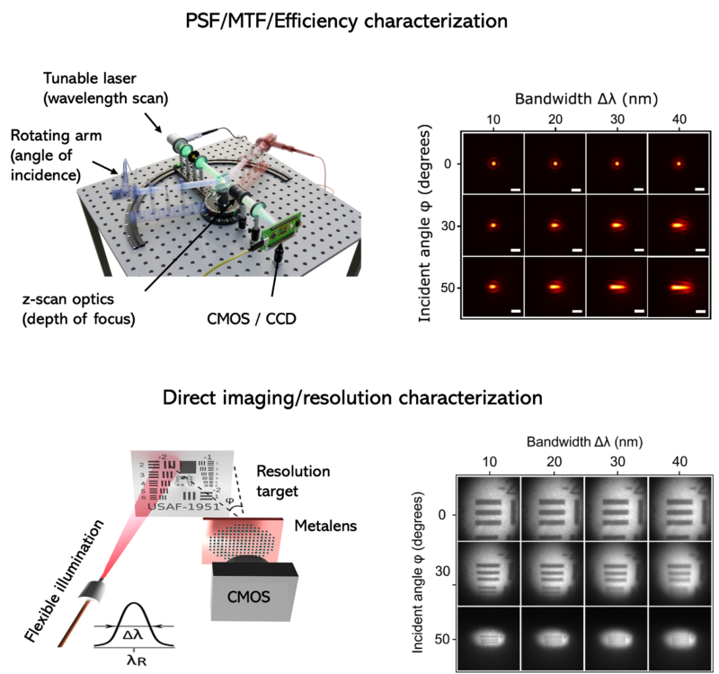
To ensure the absolute integrity and performance of every device, we conduct exhaustive characterisation using state-of-the-art equipment. NSTIC’s multi-stage process validates every aspect of the component, from its physical nanostructure to its final system-level functionality, guaranteeing it meets the most stringent design specifications.
Structural Characterisation:
- Scanning Electron Microscopy (SEM), cross-sectional Transmission Electron Microscopy (TEM), and Atomic Force Microscopy (AFM).
Optical & Performance Characterisation:
- Wide Spectrum Analysis: Full characterisation across UV, visible, near-IR, and mid-IR ranges.
- Light Interaction: Measurement of transmission and reflection spectra (down to 0.5um spatial resolution), refractive index, and transmission/reflection phase.
- Angular Performance: Angular-resolved spectroscopy and spectrally resolved back focal plane imaging.
- Imaging Quality: Focusing efficiency, Point Spread Function (PSF), and Modulation Transfer Function (MTF) characterisation at varying incident angles.
- Defect & System Validation: Quantitative phase imaging for defect inspection, full imaging performance analysis, electrical device testing, and final system performance validation.
Seamless Integration: From Components to Full Systems
Our expertise extends beyond component fabrication to the seamless integration of flat optics into larger modules and complete systems, ensuring optimal performance in real-world applications. We bridge the gap between advanced components and functional devices.
- Capability: Full optical system design and end-to-end integration
- Systems Under Development: 3D point sensors, photoacoustic microscopy, hyperspectral imaging, endoscopy, and Raman/SERS spectroscopy
Collaborative Innovation: The NSTIC Advantage in Flat Optics
As a leading translation centre for semiconductor photonics technologies, NSTIC provides a decisive advantage in collaborative innovation. Our core strength is our world-class team of researchers, whose deep expertise attracts leading talent in photonics. This intellectual capital is further amplified by access to state-of-the-art facilities, including our 300mm wafer cleanroom, which offers unmatched capabilities in the region for advanced fabrication.
We are uniquely positioned to translate ambitious research into industry-defining products, empowering partners to pioneer next-generation systems for demanding sectors like automotive sensing and high-speed data centre communication, turning innovative concepts into commercial reality.
Ready to Innovate? Connect with Our Flat Optics Experts
Whether you are exploring a new application for flat optics or wish to initiate collaboration projects to accelerate your R&D fabrication, our team is ready to assist.