Advanced Photonics: Systems, Technology & Applications
Advanced Photonics: Enabling High-Speed Optical Communication and Next-Gen Transceivers
Advanced photonics is a critical technology driving the future of high-speed optical communication, essential for powering the massive data demands of cloud and AI infrastructure. It enables the development of next-gen transceivers essential for meeting the exponential data demands of modern data centres, offering faster, more energy-efficient solutions than conventional electronics used for optical interconnections and beyond.
TABLE OF CONTENTS
- What is Advanced Photonics?
- Photonics Applications: Revolutionizing High-Speed Data Transmission
- Photonics Heterogeneous Integration (PHI): Enhancing Performance and Scalability
- Photonics Design Enablement (PDE): Enabling the Future of Photonics Systems
- Advanced Electro-Optical Testing Capability: Ensuring High-Performance Photonics Systems
- Overcoming Challenges in Current Silicon Photonics
- Exploring New Materials for Advanced Photonics
- Why NSTIC for Advanced Photonics Solutions?
- Contact NSTIC for Expert Consultation on Advanced Photonics
What is Advanced Photonics?
Advanced photonics integrates core optical components, such as waveguides, modulators, and photodetectors, onto silicon substrates to create photonic integrated circuits (PICs). As the demand for faster information processing rises, conventional electronics face significant limitations.
Photonics emerges as a crucial solution, using light for high-speed data transmission and optical interconnections. This technology offers superior processing speeds and lower energy consumption. It builds upon established semiconductor foundry processes, offering proven scalability and reliability for diverse applications—from data centre communications to quantum technologies and LiDAR systems.
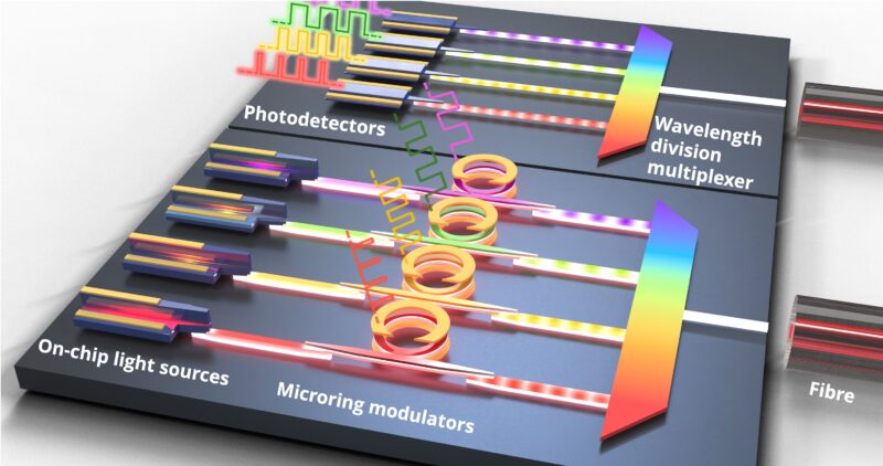
Photonics Applications: Revolutionising High-Speed Data Transmission
Photonics is fundamental to modern high-speed data communication, forming the backbone of telecommunications networks and the internal fabric of data centres. Its primary application involves optical interconnections, where data is transmitted as light through fibre optic cables, enabling faster speeds with less signal loss than traditional copper wiring.
In data centres, advanced optical transceiver technologies are crucial for managing immense traffic loads, facilitating rapid server-to-server communication. These transceivers are continuously evolving, scaling to ever-higher speeds to ensure that network infrastructure can support the exponential growth of cloud computing and AI.
Photonics Heterogeneous Integration (PHI): Enhancing Performance and Scalability
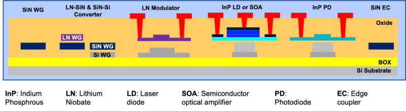
Photonic Heterogeneous Integration (PHI) is a transformative strategy that overcomes the intrinsic limitations of pure silicon. It enables the development of high-performance transceivers and optical devices by integrating superior, specialised materials onto a single silicon platform for each distinct function:
- Efficient Light Management: It utilises III-V materials for powerful light generation (lasers) and high-speed detection (photodetectors), functions where silicon is naturally inefficient.
- Ultra-Fast Modulation: It incorporates materials with a strong Pockels effect, like Lithium Niobate (LN), to achieve data modulation speeds that are impossible with silicon alone.
- Low-Loss Light Routing: This approach utilises dedicated waveguide materials to guide light across the chip with minimal signal degradation, ensuring maximum signal integrity.
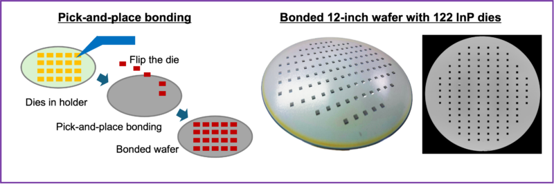
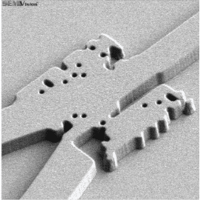
III/V-to-Si Bonding Using High-Throughput Pick-and-Place D2W Bonding
A key technique within our PHI platform is high-throughput, die-to-wafer (D2W) bonding. This advanced process allows for the precise placement and integration of small, high-performance dies of various optical materials (such as Indium Phosphide or Lithium Niobate) onto a large-format silicon wafer. This is followed by a wafer-level fabrication process using standard CMOS tools to create the final integrated circuit. This methodology yields several key advantages:
- Flexibility: Enables the ability to bond dies of different materials onto the same silicon wafer, creating multi-functional circuits.
- Scalability: The process is scalable for both 8-inch and 12-inch wafers, aligning with high-volume semiconductor manufacturing standards.
- Manufacturability: Enables post-bonding, wafer-level fabrication of integrated devices using established and reliable CMOS processes.
- Cost-Effectiveness: Ensures that expensive materials, such as III-V compounds or Lithium Niobate, are used only where their specific functions are needed, thereby optimising material costs.
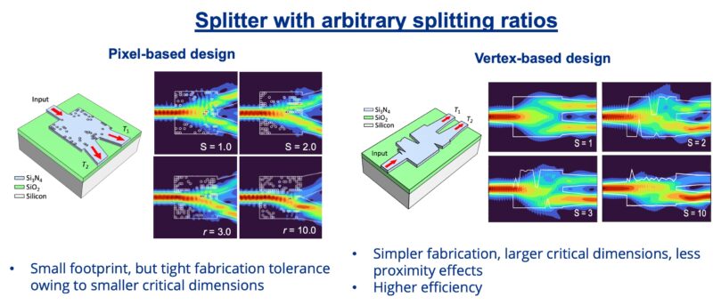
Photonics Design Enablement (PDE): Enabling the Future of Photonics Systems
Photonics Design Enablement (PDE) is a crucial framework that accelerates the creation of advanced photonics systems. It provides designers with a sophisticated suite of simulation tools, process design kits (PDKs), and validated device models.
By accurately predicting how a device will perform before manufacturing, PDE allows for rapid virtual prototyping and optimisation. This significantly reduces costly and time-consuming fabrication cycles, enabling faster innovation and development. Ultimately, this ‘first-time-right’ design approach is crucial for rapidly bringing efficient, high-performance photonic integrated circuits from concept to reality, thereby enabling advances in communications, computing, and sensing.
Photonics design enablement for next-generation application by using machine-learning based photonic design methodologies.
To push the boundaries of what is possible, we go beyond conventional design approaches by using advanced machine-learning (ML) methodologies. This allows us to rapidly simulate and optimise complex photonic devices, significantly reducing development cycles and improving final device performance.
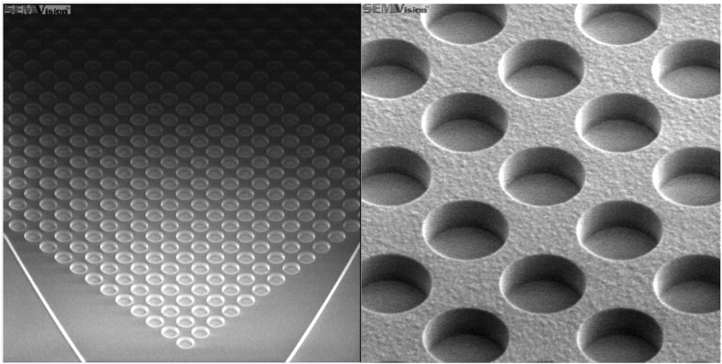
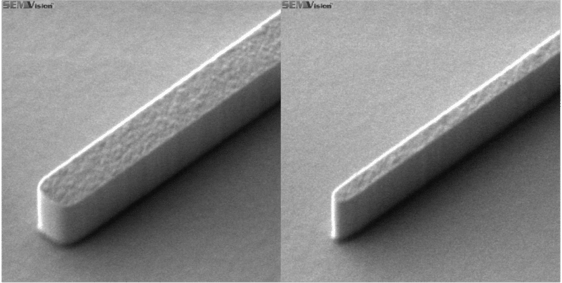
Device Fabrication
Our state-of-the-art facility brings innovative designs to life, transforming concepts into tangible realities. We perform all photonic device fabrication and demonstration using industry-grade tools to ensure maximum precision and reliability.
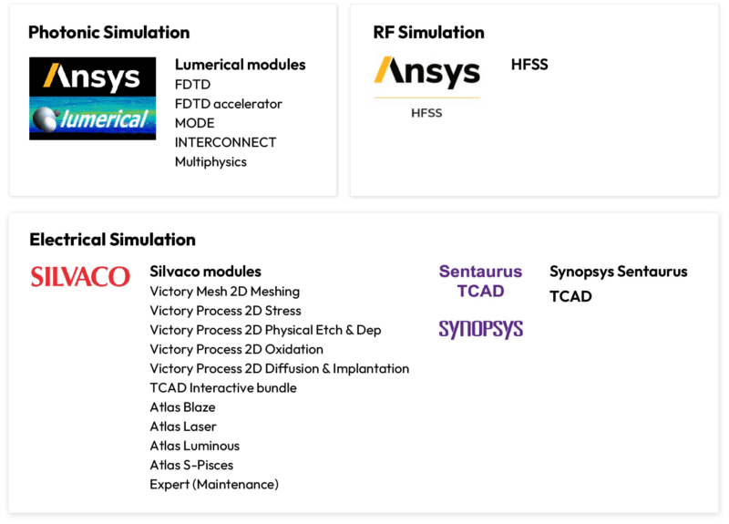
Design Software
We utilise a comprehensive suite of industry-standard design software to create and simulate advanced photonic circuits. These powerful tools enable us to ensure design accuracy and performance before the fabrication process begins.
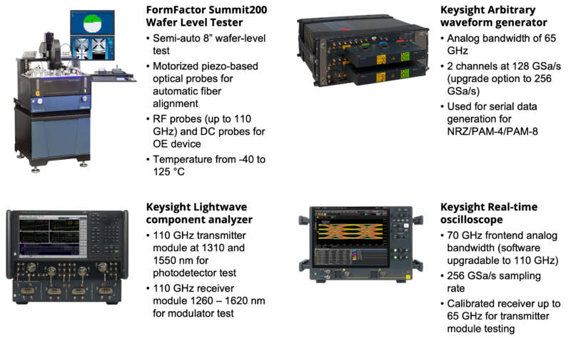
Advanced Electro-Optical Testing Capability: Ensuring High-Performance Photonics Systems
To ensure system performance, our testing capability provides rigorous validation focused on key components. The process begins with our automated wafer-level tester, which performs crucial quality assurance and functionality checks across the entire wafer before individual devices are separated.
For specific components, an arbitrary waveform generator produces complex, high-speed electrical signals to simulate real-world conditions during transmitter module testing. This allows us to verify signal integrity and speed.
Complementary photodetector tests then validate receiver performance by measuring critical parameters, such as sensitivity and response. This multi-stage approach guarantees that every component functions precisely as designed.
Fully Equipped for 200G/Lane Data Communication
To support the development of next-generation 1.6T transceivers, our testing infrastructure is fully engineered to meet the 200G-per-lane performance benchmark.
We possess the state-of-the-art equipment required for complete signal generation and characterisation at these demanding speeds.
Overcoming Challenges in Current Silicon Photonics
The material’s inherent performance limitations often challenge the scalability of conventional silicon photonics. Key obstacles include poor light emission, high temperature sensitivity, and a critical speed bottleneck in traditional silicon modulators. These issues not only restrict data rates but also increase power consumption and design complexity, hindering progress for demanding next-generation applications.
Our service overcomes these issues by strategically integrating next-generation materials onto the silicon platform. This heterogeneous integration approach uses materials with superior optical properties precisely where needed, creating powerful hybrid circuits. They effectively bypass silicon’s performance ceiling, unlocking new functionalities and delivering the efficient, advanced optical devices your applications demand.
Exploring New Materials for Advanced Photonics
To deliver a decisive performance advantage, our service harnesses a portfolio of advanced materials that overcome silicon’s inherent limitations.
We integrate leading-edge options, such as thin-film lithium niobate (TFLN) to build ultra-high-speed modulators essential for next-generation transceivers We also leverage barium titanate (BTO) for its potential in creating highly efficient, low-power photonic devices suitable for large-scale systems.
For systems requiring minimal optical loss for complex light routing or advanced nonlinear effects, we utilise materials such as aluminium nitride (AlN). By expertly integrating these specialised materials onto a silicon platform, our hybrid photonic approach allows us to develop the customised, high-performance devices your applications require to succeed.
Why NSTIC for Advanced Photonics Solutions?
NSTIC Singapore is your dedicated research and development partner for navigating the complexities of advanced photonics. We offer unparalleled expertise and state-of-the-art capabilities to solve the industry’s most pressing challenges, turning your innovative concepts into viable, high-performance devices and manufacturable prototypes ready for commercialisation.
Our unique strengths lie in two critical areas:
- Photonic Heterogeneous Integration (PHI): We are experts at strategically integrating novel, non-silicon materials onto a silicon platform. This capability allows us to overcome the inherent limitations of conventional silicon, creating powerful hybrid devices with superior speed, efficiency, and functionality that would otherwise be unachievable.
- Photonics Design Enablement (PDE): Our advanced design and simulation frameworks, including machine-learning methodologies, significantly de-risk and accelerate your development cycle. By modelling device performance with high accuracy before fabrication, we enable first-time-right prototyping, saving valuable time and resources.
Partnering with NSTIC means leveraging our world-class R&D engine to validate your designs and build high-performance demonstrators. We de-risk your project and create a seamless pathway to commercialisation by providing foundry-ready processes for your most advanced photonic solutions.
Contact NSTIC for Expert Consultation on Advanced Photonics
Let’s build the future of photonics together. Work with us and explore our research and development partnerships and expert consultation opportunities.