-
State-of-the-art Class 10/100 cleanroom and lab space
-
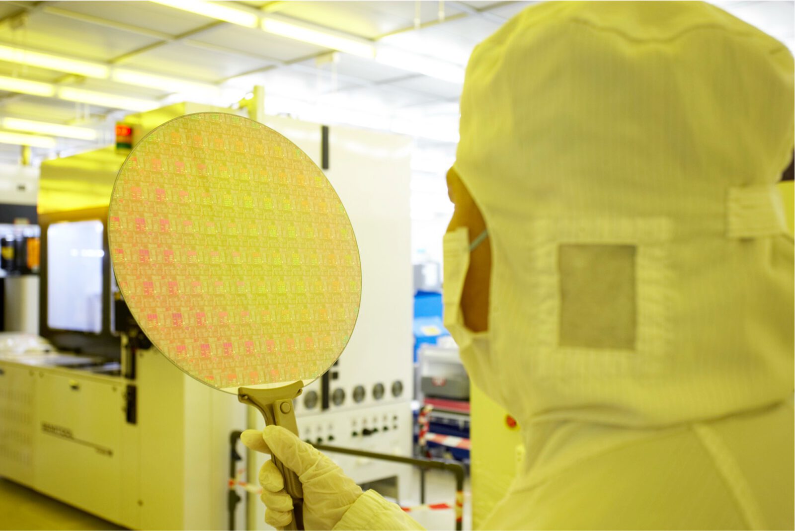
8” / 12” silicon and 12″ glass wafer processing
-
Supports R&D, single/multi process run, prototyping to small volume fabrication with automated industry-ready tools
-
Full suite of fabrication tools
Lithography
- ArF immersion scanner (>45 nm L/S)
- KrF scanner (>110nm L/S)
- GHI-line stepper (>0.8μm L/S)
Dry Etch/Dry Strip
- Si/SiOx/a-Si high aspect ratio etch (up to 1:10)
- SiN, III-V, Lithium Niobate etch
- N2, O2, forming gas strip
- Descum
Wet Etch/Cleans
- Bench and single wafer frontside and backside particle cleans
- Post-etch residue removal and PR strip
- Cu, Ti, Si, oxide wet etch
Thin Films
- PVD sputtering: Ti, TiN, Ta, TaN, Cu, Al, Ni, AlN, ScAlN, SiN
- PVD evaporation: Au, Ti, Al, Ni, Cr
- PECVD: Low-stress TEOS, SiOx, SiN, a-Si
- ALD: TiN, HfOx, AlN, Al2O3, TiO2
Diffusion/Implant
- LPCVD: SiN, N+ poly Si, LPTEOS
- SiC, Ge, Si, SiGe epitaxy
- B, P, Al, N ion implantation
- Thermal oxidation (up to 1250 0°C)
- Implant activation (up to 2000 0°C)
CMP
- SiOx, SiN, Si
- Cu, barrier
Electroplating
- Cu TSV (high aspect ratio up to 1:15)
- Cu damascene, RDL
- Au, Ni, SnAg
Advanced Packaging
- Wafer-to-wafer fusion/hybrid bonding (with overlay accuracy 3σ <100 nm)
- Chip-to-wafer pick-and-place bonding
- Si-Si, Si-glass temporary bonding and debonding
- Mechanical dicing
- Si, glass backgrinding
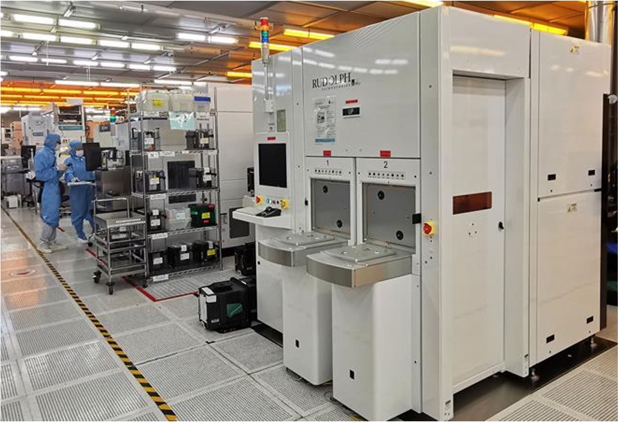
Metrology and Inspection
- Micro and macro defect optical inspection
- Defect review SEM with EDX
- CDSEM, overlay metrology
- 3D optical profiler
- Surface roughness/morphology by 2D/3D AFM
- Dielectric and metal thickness metrology
- Confocal scanning acoustic microscopy
- Optical probe station